

Weekly Quiz CompetitionSHARING IS CARING
If our Website helped you a little, then kindly spread our voice using Social Networks. Spread our word to your readers, friends, teachers, students & all those close ones who deserve to know what you know now.


Correct -
Wrong -
Skipped -


 ×
×
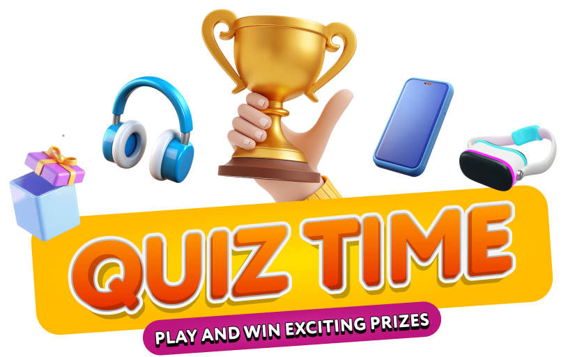
"Log in, submit answer and win prizes"
"Enter your details to claim your prize if you win!"
Provide prime members with unlimited access to all study materials in PDF format.
Allow prime members to attempt MCQ tests multiple times to enhance their learning and understanding.
Provide prime users with access to exclusive PDF study materials that are not available to regular users.


Thank you for participating in Quiz Time!
Good luck, and stay tuned for exciting rewards!
Your Selected Class:
Your Selected Stream:


 Sign in
 Profile
 Signout